
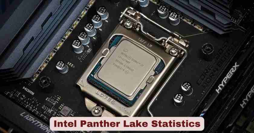
What Is Intel Panther Lake?
Intel Panther Lake — officially launched as the Intel Core Ultra Series 3 processor family on January 5, 2026 at CES 2026 in Las Vegas — is one of the most significant chips Intel has produced in over a decade, and arguably the most strategically important product the company has shipped since it began rebuilding its manufacturing credibility. At its core, Panther Lake is a mobile system-on-chip (SoC) designed to power laptops, mini PCs, handheld gaming devices, edge computing systems, and industrial applications. But beyond the spec sheet, it is something else entirely: it is the first client processor ever built on Intel’s proprietary 18A process node, the most advanced semiconductor manufacturing technology developed and manufactured on American soil. Every CPU tile inside a Panther Lake chip is fabricated at Fab 52, Intel’s newest high-volume production facility on its Ocotillo campus in Chandler, Arizona — a facility that Intel describes as producing the most advanced logic chips in the United States, and that represents a portion of Intel’s $100 billion commitment to expanding domestic semiconductor operations. The 18A node introduces two technologies that Intel has been developing for years: RibbonFET, Intel’s gate-all-around transistor architecture (its first new transistor design in over a decade), and PowerVia, a backside power delivery system that separates power distribution from signal routing to reduce voltage droop by approximately 10% and deliver frequency gains of up to 10% at equivalent power levels.
The performance and efficiency story that Panther Lake tells at launch is the one Intel’s partners, investors, and customers have been waiting to hear for several years. Marketed under the Core Ultra Series 3 branding — with the new Core Ultra X9 and Core Ultra X7 designations reserved for the highest-tier configurations featuring 12 Xe3 GPU cores — the platform delivers, according to Intel’s own benchmarks at CES 2026, up to 60% better multithreaded CPU performance vs Lunar Lake, up to 77% better gaming performance vs Lunar Lake, up to 180 total platform TOPS for AI workloads, and battery life extending to 27 hours for video streaming. The flagship Core Ultra X9 388H chip packs 16 cores (4 Cougar Cove P-cores + 8 Darkmont E-cores + 4 low-power E-cores) clocked up to 5.1 GHz, 12 Xe3 GPU cores in the Arc B390 integrated GPU, and a 25W base TDP with up to 80W maximum turbo power. Retail laptop availability began on January 27, 2026, with over 200 system designs from partners including Lenovo, Asus, Acer, Dell, and HP already confirmed. The platform has been widely described as a “return to form” for Intel in the mobile space — combining the efficiency heritage of Lunar Lake with the scalable performance range that Arrow Lake provided in a single, cohesive, entirely Intel-manufactured package.
Interesting Facts About Intel Panther Lake 2026
Here are the most striking and verified facts about Intel Panther Lake (Core Ultra Series 3) — drawn from Intel’s official CES 2026 announcements, the Intel Newsroom, Neowin, HotHardware, PCWorld, NotebookCheck, Phoronix, VideoCardz, WCCFtech, and Wikipedia as of April 7, 2026.
| # | Fact | Detail |
|---|---|---|
| 1 | Official name | Intel Core Ultra Series 3 — codename Panther Lake |
| 2 | Launch event and date | CES 2026, January 5, 2026 — Las Vegas, presented by Jim Johnson, Intel SVP and GM of Client Computing Group |
| 3 | Retail availability date | January 27, 2026 — global laptop retail rollout |
| 4 | Process node | Intel 18A — 1.8nm-class; first client SoC ever built on Intel 18A; most advanced semiconductor process developed and manufactured in the United States |
| 5 | Key transistor technology | RibbonFET — Intel’s Gate-All-Around (GAA) transistor; first new transistor architecture from Intel in over a decade |
| 6 | Power delivery technology | PowerVia — backside power delivery; reduces voltage droop by ~10%, enables frequency gains of up to 10% at same power |
| 7 | Manufacturing facility | Fab 52 — Intel’s fifth high-volume fab at its Ocotillo campus in Chandler, Arizona |
| 8 | Intel US investment | Fab 52 is part of Intel’s $100 billion commitment to expand domestic semiconductor operations |
| 9 | Process advantage vs Intel 3 | Intel 18A delivers 15% better efficiency and 30% better density vs Intel’s previous Intel 3 process — HotHardware |
| 10 | Flagship SKU | Core Ultra X9 388H — 16 cores (4P+8E+4LPE), 12 Xe3 GPU cores, up to 5.1 GHz boost, 25W base TDP, 80W turbo |
| 11 | CPU performance claim | Up to 60% faster multithreaded performance vs Lunar Lake at similar power (Cinebench 2024 MT, 25W) |
| 12 | Gaming performance claim | Up to 77% better gaming vs Lunar Lake (geomean across 45 game titles at 1080p High with 2x upscaling) |
| 13 | AI performance | Up to 180 total Platform TOPS (120 from GPU + 50 from NPU) |
| 14 | Battery life claim | Up to 27 hours Netflix streaming; up to 17 hours office productivity — Intel CES 2026 |
| 15 | OEM system designs | Over 200 system designs confirmed from global OEM partners at launch |
| 16 | Arc B390 iGPU gaming | Performance approaching NVIDIA GeForce RTX 4050 Laptop GPU territory at 45W TDP (12 Xe3 cores, 2.5 GHz) |
| 17 | Memory support (flagship) | LPDDR5X-9600 MT/s and DDR5-7200; up to 96 GB LPDDR5X or 128 GB DDR5 DIMM |
| 18 | Handheld gaming launch | Intel confirmed dedicated handheld gaming SKUs (G-series) based on Panther Lake, coming later in 2026 — TechRadar |
| 19 | Server 18A chip | Clearwater Forest (Xeon 6+) — Intel’s first 18A server processor; up to 288 E-cores; launched H1 2026 |
| 20 | TSMC 2nm comparison | Intel 18A reached high-volume manufacturing ahead of TSMC’s N2 (2nm) schedule, which is not expected at similar volume until mid-to-late 2026 |
Source: Intel Newsroom — CES 2026 launch (January 5, 2026); Intel Newsroom — Panther Lake architecture reveal (October 9, 2025); Neowin — Intel Core Ultra 300 launch coverage (January 5, 2026); HotHardware — Panther Lake performance at CES 2026; PCWorld — Core Ultra X9 388H review (January 26, 2026); NotebookCheck — Core Ultra X9 388H specs; Phoronix — CES 2026 keynote notes; VideoCardz — Panther Lake specs (October 2025); WCCFtech — Core Ultra Series 3 launch coverage (January 2026); Wikipedia — Panther Lake microprocessor; TechRadar — Intel 2026 plans interview; Tom’s Hardware — Fab 52 analysis; Financial Content — 18A HVM milestone (January 2026)
What makes Panther Lake genuinely significant — beyond the spec numbers, which every chip generation delivers — is the combination of manufacturing independence and performance balance that Intel has been chasing for half a decade. The “five nodes in four years” programme that former CEO Pat Gelsinger announced as Intel’s foundry rescue plan was widely treated with scepticism when it launched. The industry had watched Intel stumble badly through the 10nm and 7nm transitions, and there was real doubt about whether any company could simultaneously redesign its manufacturing process and ship competitive products on it. Panther Lake is the answer to that doubt. It is not only shipping on 18A — it is shipping on 18A with over 200 OEM system designs at launch, with battery life claims that rival ARM-based competitors, and with integrated graphics performance that has reviewers declaring it genuinely competitive with entry-level discrete GPUs. That combination, if it holds up under independent testing at scale, represents a genuine turning point for Intel.
The decision to manufacture the CPU tile entirely in-house at Fab 52 in Arizona is also strategically significant beyond Intel’s internal economics. The US CHIPS Act — which Congress passed partly to incentivise exactly this kind of domestic semiconductor investment — gets its clearest validation in Panther Lake. Intel is producing what it calls the most advanced consumer chip node in the world, on US soil, in volume, before TSMC’s equivalent N2 process reaches comparable output. That is not a statement Intel could have made at any point in the previous five years.
Intel Panther Lake Architecture and Process Technology Statistics 2026
| Architecture / Process Parameter | Data |
|---|---|
| Codename | Panther Lake |
| Product branding | Intel Core Ultra Series 3 (Core Ultra 300 series) |
| Generation | 3rd generation Core Ultra; successor to Lunar Lake (Series 2) and extends beyond Arrow Lake |
| Process node — CPU tile | Intel 18A (1.8nm-class) — manufactured at Fab 52, Chandler, Arizona |
| Process node — GPU tile | Intel 3 or TSMC N3E depending on configuration |
| Process node — I/O / platform controller tile | TSMC N6 |
| Chip architecture | Multi-tile / chiplet design using Foveros-S advanced 3D packaging |
| CPU tiles in flagship (H-series) | 4P + 8E + 4LPE = 16 total cores (no Hyper-Threading) |
| CPU tiles in entry-level | 4P + 4LPE = 8 total cores |
| P-core architecture | Cougar Cove — new Intel P-core design |
| E-core architecture | Darkmont — new Intel E-core design |
| LP-E core architecture | Darkmont (low-power variant) |
| Transistor technology | RibbonFET — Gate-All-Around (GAA); Intel’s first new transistor design in over a decade |
| Power delivery | PowerVia — backside power delivery; ~10% voltage droop reduction; up to 10% frequency gain at same power |
| Packaging technology | Foveros-S — 3D chip stacking combining CPU, GPU, and I/O dies |
| Integrated GPU architecture | Xe3 “Celestial” — successor to Xe2 Battlemage |
| NPU generation | NPU5 (5th generation) |
| 18A vs Intel 3 (density) | 30% better density — HotHardware, Intel CES 2026 data |
| 18A vs Intel 3 (efficiency) | 15% better efficiency |
| Intel 18A market position | First and only GAA + backside power delivery combo in high-volume consumer production globally as of CES 2026 |
| TSMC N2 comparison | TSMC N2 not expected at comparable volume until mid-to-late 2026 — Financial Content (December 2025) |
| Foundry customers on 18A | Microsoft and Amazon committed to using 18A for custom AI silicon |
Source: Intel Newsroom — Panther Lake architecture reveal (October 9, 2025); Intel Newsroom — CES 2026 launch (January 5, 2026); Wikipedia — Panther Lake microprocessor; HotHardware — CES 2026 Panther Lake performance launch; VideoCardz — Panther Lake tile design specs (October 2025); Financial Content / WRAL — 18A HVM milestone (December 2025 and January 2026); WCCFtech — Core Ultra Series 3 architecture deep dive; Pokde.net — CES 2026 Intel coverage (January 7, 2026)
The multi-tile architecture of Panther Lake is one of the most sophisticated chiplet designs Intel has ever shipped in a consumer product, and understanding it is key to understanding both the platform’s performance profile and Intel’s strategic direction. Unlike monolithic SoCs — where every functional block sits on a single die — Panther Lake separates its functions across three distinct tiles, each manufactured on the process node best suited to it. The CPU compute tile, where performance is most sensitive to transistor quality and density, uses Intel’s proprietary 18A node. The GPU tile, where the design is derived from existing IP and power delivery is less critical, uses either Intel 3 or TSMC N3E depending on the configuration tier. The I/O and platform controller tile, which handles connectivity rather than computation, uses the cost-efficient TSMC N6. These tiles are then assembled into a single package using Foveros-S stacking, which Intel has been refining since Lakefield.
The RibbonFET and PowerVia combination that defines Intel 18A is genuinely unprecedented in commercial production. Every major chipmaker is moving toward gate-all-around transistors — TSMC with its N2 node, Samsung with its 3GAE — but none of them have combined GAA with backside power delivery in a product shipping to consumers. Backside power delivery removes the power distribution network from the front side of the wafer, which has historically competed with signal routing for space and caused routing congestion. Moving it to the back frees up the front for more signal lines, reduces electrical interference, and allows transistors to be packed more densely. The practical result, as Intel quantifies it, is a 10% reduction in voltage droop and up to a 10% frequency gain at the same power level — modest numbers individually, but compounding across millions of transistors in a chip with over 100 billion transistors in the compute tile alone.
Intel Panther Lake Core Ultra Series 3 SKU Specifications 2026
| SKU | Cores | Max Boost | Xe3 GPU Cores | NPU TOPS | Base TDP | Max Turbo Power | Memory Support |
|---|---|---|---|---|---|---|---|
| Core Ultra X9 388H | 16 (4P+8E+4LPE) | 5.1 GHz | 12 (Arc B390) | 50 | 25W | 65–80W | LPDDR5X-9600, DDR5; up to 96 GB |
| Core Ultra X7 358H | 16 (4P+8E+4LPE) | Up to ~4.8 GHz | 12 (Arc B390) | 50 | ~25W | ~65–80W | LPDDR5X-9600, DDR5; up to 96 GB |
| Core Ultra 9 386H | 16 (4P+8E+4LPE) | ~4.8–5.0 GHz | 4 | 50 | ~25W | ~65–80W | LPDDR5X, DDR5; up to 128 GB |
| Core Ultra 7 366H | 16 | ~4.5–4.8 GHz | 4 | 50 | ~25W | ~65W | LPDDR5X, DDR5 |
| Core Ultra 7 356H | 16 | ~4.3–4.7 GHz | 4 | 50 | ~25W | ~65W | LPDDR5X, DDR5 |
| Core Ultra 5 338H | 16 | ~4.0 GHz | 4 | 50 | ~25W | ~65W | LPDDR5X, DDR5 |
| Core Ultra 5 336H | 16 | ~3.8 GHz | 4 | 50 | ~25W | ~60W | LPDDR5X, DDR5 |
| Core Ultra 7 365 | 8 (4P+4LPE) | ~4.5 GHz | 4 | 50 | ~17W | ~37W | LPDDR5X-6800, DDR5-6400; up to 128 GB |
| Core Ultra 7 355 | 8 | ~4.3 GHz | 4 | 50 | ~17W | ~37W | LPDDR5X, DDR5 |
| Core Ultra 5 325 | 8 | ~4.0 GHz | 4 | 50 | ~17W | ~37W | LPDDR5X, DDR5 |
| Core Ultra 5 322 | 8 | ~3.8 GHz | 4 | 50 | ~17W | ~37W | LPDDR5X, DDR5 |
| Total SKUs at launch | 14 SKUs confirmed across the Panther Lake lineup |
Source: Intel official product page — Core Ultra X9 388H specifications (intel.com); Phoronix — CES 2026 keynote SKU details (January 5, 2026); WCCFtech — Panther Lake launch coverage (January 2026); VideoCardz — Panther Lake SKU details (October 2025); NotebookCheck — Core Ultra X9 388H processor specs; Ultrabook Review — Panther Lake SKU breakdown (January 27, 2026); HotHardware — Core Ultra X9 388H review (January 26, 2026)
The introduction of the “X” prefix naming convention is one of the most important marketing and product differentiation decisions Intel has made with Panther Lake. Core Ultra X9 and Core Ultra X7 SKUs denote chips with the full 12 Xe3 core Arc B390 GPU — the configuration that delivers the headline gaming performance claims. The non-X H-series models use the 4 Xe3 core GPU tile instead, targeting the mainstream productivity segment where integrated graphics demands are more modest. This segmentation allows Intel to meet two very different markets with the same underlying platform architecture: power users who want near-discrete gaming capability from integrated graphics (X9/X7), and enterprise and professional users who want outstanding efficiency and battery life above all else (standard H-series and U-series). The ability to offer both from a single chipset family — just by selecting different GPU tiles — is exactly the kind of scalability that Intel’s multi-tile architecture was designed to enable.
The 8-core entry-level configuration (Core Ultra 7 365, Core Ultra 5 325, Core Ultra 5 322, etc.) represents Panther Lake’s direct replacement for Lunar Lake in the thin-and-light segment. These chips use the smaller 4P + 4LPE core tile without the mid-level Darkmont E-core cluster, running at lower base TDPs (around 17W) and with more conservative memory bandwidth support (LPDDR5X-6800 vs the H-series’ 9600 MT/s). For business-focused ultrabooks prioritising all-day battery life and slim form factors, this configuration is the sweet spot — and Intel’s TechRadar interview confirms that these 8-core models are specifically designed to deliver 20+ hours of battery life even in the most basic configurations, which would represent a meaningful competitive counter to Qualcomm’s Snapdragon X platform in the ARM-based efficiency laptop segment.
Intel Panther Lake Performance Benchmarks Statistics 2026
| Benchmark / Performance Metric | Result / Claim | Comparison |
|---|---|---|
| Multithreaded CPU performance | Up to 60% better vs Lunar Lake Core Ultra 9 288V at same power | Cinebench 2024 Multi Core at 25W — Intel CES 2026 |
| Single-threaded performance | ~10% better vs Lunar Lake and Arrow Lake at same power — or same performance at 40% less power | VideoCardz (October 2025) |
| Multithreaded at Arrow Lake power | Up to 30% lower power at Arrow Lake-equivalent performance | VideoCardz (October 2025) |
| Gaming vs Lunar Lake (Arc B390) | Up to 77% better gaming across 45 game titles at 1080p High with 2x upscaling | Intel CES 2026 official benchmark |
| Gaming vs AMD Strix Point | 73% better performance on average with Arc B390 — Intel claim | Pokde.net CES 2026 |
| iGPU vs RTX 4050 Laptop GPU | Arc B390 (12 Xe3, 45W) approaches performance equivalence with RTX 4050 Laptop at 60W TGP | Pokde.net; NotebookCheck |
| Battery life — video streaming | Up to 27 hours (Netflix) — Intel CES 2026 claim | Confirmed ~22+ hours in ASUS Zenbook Duo real-world test (99Wh battery) — WCCFtech |
| Battery life — office productivity | Up to 17 hours — Intel CES 2026 | |
| AI performance — total platform TOPS | Up to 180 TOPS (120 GPU + 50 NPU + 10 CPU) | |
| NPU5 INT8 performance | 50 TOPS — matches AMD Ryzen AI 300; below Qualcomm’s 80 TOPS but faster in LLM inference | |
| LLM inference vs AMD XDNA2 | Intel NPU5: 4.3x faster LLM inference than AMD XDNA2 (Ryzen AI 9 HX 370) — Intel claim | HotHardware CES 2026 |
| NPU5 vs Core Ultra 9 285H NPU | 2x faster than NPU3 in the Core Ultra 9 285H (Arrow Lake) | HotHardware |
| Geekbench 6 — X9 388H single-core | 3,057 points — early engineering sample leak | Tom’s Hardware (December 2025) |
| Geekbench 6 — X9 388H multi-core | 17,687 points — early engineering sample leak | Tom’s Hardware (December 2025) |
| X9 388H vs Ryzen AI Max+ 395 (SC) | 8.7% faster single-core at a 45W TDP vs 55W for AMD — Tom’s Hardware | |
| Cinebench 2024 — single-core | 130 points — top single-core score at launch — WCCFtech review | |
| Cinebench 2024 — multithreaded vs 285H | 43% faster multithreaded than Arrow Lake Core Ultra 9 285H — WCCFtech | |
| 3DMark gaming boost with AI upscaling | Cyberpunk 2077: 52 fps → 92 fps with AI frame generation — PCWorld review |
Source: Intel Newsroom — CES 2026 launch performance claims (January 5, 2026); HotHardware — CES 2026 Panther Lake coverage and X9 388H review (January 2026); PCWorld — Core Ultra X9 388H review (January 26, 2026); Tom’s Hardware — X9 388H Geekbench leak (December 2025); WCCFtech — ASUS Zenbook Duo X9 388H review (February 2026); VideoCardz — Panther Lake performance specs (October 2025); Pokde.net — CES 2026 Intel coverage; Phoronix — CES 2026 keynote
The benchmark numbers for Panther Lake tell a more nuanced story than Intel’s headline claims alone. The 60% multithreaded improvement over Lunar Lake is real in the Cinebench test — but Lunar Lake was a deliberately constrained, 8-core efficiency chip, so the comparison is partly a product of the much higher core count in Panther Lake’s flagship H-series. The more meaningful competitive comparison is against Arrow Lake (Core Ultra 9 285H), and here the picture is impressive for a different reason: Panther Lake’s X9 388H is 43% faster in multithreaded Cinebench while drawing comparable power — that is, it wins on both performance and efficiency simultaneously, which is exactly what Intel needed to claim after Arrow Lake’s mixed critical reception. The 8.7% single-core advantage over AMD’s Ryzen AI Max+ 395 at a 10W lower TDP is the comparison that will matter most to the competitive landscape.
The Arc B390 integrated graphics story is perhaps the most commercially transformative aspect of Panther Lake, because it directly attacks the assumption — which has been embedded in laptop purchasing decisions for years — that you need a discrete GPU to play modern games. PCWorld’s conclusion that AI-assisted frame generation brings Cyberpunk 2077 from 52 fps to 92 fps on integrated graphics is the kind of result that will generate real buying decisions. NotebookCheck’s finding that the Arc B390 is ~70% faster than previous-gen Intel iGPUs and approaches RTX 4050 Laptop territory is even more striking. For a thin-and-light laptop or a future handheld gaming device running purely on integrated graphics, that level of performance opens up a category of games and workloads that was simply inaccessible to previous integrated graphics solutions. Whether Intel can sustain this advantage when AMD refreshes its Strix Halo line and Qualcomm’s competing solutions arrive will define the competitive landscape for the next 18 months.
Intel Panther Lake Fab 52 and 18A Manufacturing Statistics 2026
| Manufacturing Parameter | Data |
|---|---|
| Fab name | Fab 52 — Intel’s fifth high-volume fab at Ocotillo campus |
| Fab location | Chandler, Arizona, United States |
| 18A HVM milestone | High-volume manufacturing confirmed Q4 2025 / January 2026 |
| Intel US investment total | $100 billion committed to expand domestic semiconductor operations |
| 18A process full name | Intel 18A (1.8nm-class angstrom-era node) |
| 18A angstrom measurement context | 10 angstroms = 1 nanometer; Intel switched from nanometer to angstrom-based naming with Intel 20A |
| 18A transistor architecture | RibbonFET — Gate-All-Around (GAA); replaces 10+ year FinFET standard |
| 18A power delivery | PowerVia — world’s first GAA + backside power delivery combination in consumer high-volume production |
| RibbonFET voltage droop improvement | ~10% reduction in voltage droop |
| RibbonFET frequency gain | Up to 10% at equivalent power levels |
| Intel 18A vs TSMC N2 timeline | Intel 18A at HVM before TSMC N2 reaches comparable volume (TSMC N2 expected mid-to-late 2026) |
| Fab 52 vs TSMC Arizona (Fab 21) | Intel Fab 52 capacity comparable to both TSMC Fab 21 Phase 1 and Phase 2 combined — CNBC report (Tom’s Hardware) |
| Fab 52 process sophistication | More advanced than TSMC Fab 21 Phase 1 and Phase 2 — Tom’s Hardware (December 2025) |
| 18A foundry customers committed | Microsoft and Amazon confirmed; using 18A for custom AI silicon |
| Production states | Arizona (Fab 52) and Oregon — 18A ramping in both states |
| 18A yield target | Analysts project yields to hit 70% target by early 2027 |
| Next node after 18A | Intel 14A (1.4nm) — introduces High-NA EUV; risk production expected late 2026 or early 2027 |
| Products on 18A | Panther Lake (client) and Clearwater Forest / Xeon 6+ (server, H1 2026) — first two; 18A forms foundation for at least 3 generations of Intel products |
| 18A in CHIPS Act context | Panther Lake / Fab 52 cited as validation of US CHIPS Act strategy for domestic semiconductor leadership |
Source: Intel Newsroom — Panther Lake architecture reveal (October 9, 2025); Intel Newsroom — CES 2026 launch (January 5, 2026); Data Center Dynamics — Fab 52 operational status (October 2025); Tom’s Hardware — Fab 52 vs TSMC Arizona comparison (December 2025); Financial Content / WRAL — 18A HVM milestone (December 2025); Financial Content — Silicon Renaissance analysis (January 2026); RCR Wireless — Intel 18A research note (October 2025); All About Industries — Fab 52 production launch
Fab 52 is not just Intel’s newest factory — it is the clearest physical embodiment of a geopolitical and economic strategy that has been building for years. The US CHIPS Act, signed into law in August 2022, allocated over $52 billion for semiconductor manufacturing and research in the United States, with Intel as one of its primary intended beneficiaries. The practical result of that legislation, combined with Intel’s own $100 billion domestic investment commitment, is now visible in the form of a working production facility in Chandler, Arizona, manufacturing the most advanced consumer chips in the world — a capability that until very recently existed only in Taiwan and South Korea. The CNBC report cited by Tom’s Hardware that Fab 52’s capacity is comparable to both phases of TSMC’s Arizona Fab 21 combined underlines that Intel’s domestic manufacturing footprint is not a token gesture but a genuinely competitive industrial operation.
The Microsoft and Amazon commitments to use Intel 18A for custom AI silicon are commercially significant in a way that goes beyond the revenue those contracts represent. When the two largest cloud computing companies in the world — which have historically relied almost entirely on TSMC for their most advanced custom silicon — choose to place bets on Intel’s foundry capability, it signals industry confidence in Intel 18A’s viability as an external foundry node. Intel has been building its Intel Foundry Services (IFS) division specifically to attract exactly these kinds of customers, and the Panther Lake launch provides the proof-of-concept that IFS needed: 18A works, it ships, and it works at volume. The path from that demonstration to a diversified foundry business serving multiple external customers is long, but Panther Lake represents the first major step along it.
Intel Panther Lake vs Competitors Statistics 2026
| Comparison Parameter | Panther Lake (Core Ultra X9 388H) | AMD Ryzen AI Max+ 395 | Qualcomm Snapdragon X Elite | Apple M4 (10-core) |
|---|---|---|---|---|
| Platform | Intel 18A (GAA + backside power) | TSMC N4P (FinFET) | TSMC N4P | TSMC N3E |
| CPU architecture | Hybrid x86 (Cougar Cove P + Darkmont E) | AMD Zen 5 (x86) | ARM Oryon | ARM (P-core + E-core) |
| Total CPU cores (flagship) | 16 (4P + 8E + 4LPE) | 16 | 12 | 10 (4P + 6E) |
| Max CPU boost | 5.1 GHz | ~5.1 GHz | ~4.0 GHz | ~4.4 GHz |
| Integrated GPU cores (top) | 12 Xe3 (Arc B390) | 40 RDNA 3.5 CUs | 12 Adreno | 10-core GPU |
| iGPU gaming (vs RTX 4050 tier) | Approaches RTX 4050 at 45W | Approaches RTX 4070 | Competitive at efficiency | Strong |
| Total AI TOPS | 180 TOPS (120 GPU + 50 NPU) | 50 NPU TOPS | 80 NPU TOPS | 38 NPU TOPS |
| NPU TOPS | 50 TOPS (NPU5) | 50 TOPS (XDNA2) | 80 TOPS | 38 TOPS |
| LLM inference vs AMD NPU | 4.3x faster NPU inference vs AMD XDNA2 (Intel claim) | Baseline | — | — |
| Base TDP (H-tier) | 25W | 55W (default) | ~45W | ~28–30W (est.) |
| Battery life (flagship) | Up to 27 hours streaming | ~18–20 hours (est.) | ~22 hours (est.) | ~20 hours |
| Memory support | LPDDR5X-9600 / DDR5 / up to 128 GB DIMM | LPDDR5X (up to 128 GB) | LPDDR5X | LPDDR5X |
| Max memory (H-flagship) | 96 GB (12-Xe3 config) | 128 GB | 64 GB | 32 GB |
| Connectivity | Wi-Fi 7 (R2), Bluetooth 6.0, Thunderbolt 4 | Wi-Fi 7, BT 5.3 | Wi-Fi 7, BT 5.4 | Wi-Fi 7, BT 5.3 |
| Manufacturing location | USA (Chandler, Arizona — Fab 52) | Taiwan (TSMC) | Taiwan (TSMC) | Taiwan (TSMC) |
Source: Pokde.net — CES 2026 Panther Lake competitive benchmarks; Tom’s Hardware — X9 388H vs Ryzen AI Max+ 395 Geekbench comparison (December 2025); HotHardware — CES 2026 Panther Lake AI performance slides; NotebookCheck — Core Ultra X9 388H specifications; PCWorld — X9 388H review; Intel CES 2026 official performance comparisons; WCCFtech — Panther Lake competitive positioning
The competitive comparison table reveals something important about Panther Lake’s positioning that Intel has been careful to cultivate. It is not claiming to win every single benchmark against every competitor — AMD’s Ryzen AI Max 395 still has the bigger GPU CU count and wider memory bus in its Strix Halo design, and Qualcomm’s Snapdragon X platform still offers better battery life when memory is normalised. What Panther Lake claims is to be the first platform that delivers competitive performance on every axis simultaneously in the thin-and-light laptop segment: competitive CPU performance, competitive integrated graphics, competitive AI acceleration, competitive battery life, and — critically — competitive across all of these at the same time in the same platform, rather than trading one off against another. Intel’s product leader Nish Neelalojanan’s quote to TechRadar sums up the design philosophy precisely: Panther Lake brings “Lunar Lake and Arrow Lake performance all into one place.”
The geopolitical and supply chain dimension of the comparison is worth noting explicitly. Every competing platform in this table is manufactured in Taiwan by TSMC. Panther Lake’s compute tile is manufactured in Chandler, Arizona by Intel. In a world where geopolitical risk around Taiwan’s semiconductor concentration has become a mainstream concern for governments, enterprises, and hyperscalers, that single data point has commercial and strategic implications that go well beyond benchmark scores. It is why Microsoft and Amazon have committed to 18A-based designs — not just because of Intel’s performance claims, but because domestic US manufacturing of leading-edge chips serves their own supply chain resilience goals.
Intel Panther Lake OEM Partners, Systems and Market Statistics 2026
| OEM / Market Parameter | Data |
|---|---|
| System designs confirmed at launch | Over 200 designs from global OEM partners — Intel CES 2026 |
| Pre-order availability | January 6, 2026 — pre-orders for consumer laptops opened same day as CES announcement |
| Retail availability | January 27, 2026 — global retail rollout begins |
| OEM partners confirmed | Lenovo, Asus, Acer, Dell, HP among major launch partners |
| Lenovo Panther Lake SKUs | ThinkPad X1 Carbon Gen 14 (X7), ThinkPad X9 15p (X9 388H), Yoga Slim 7i Ultra, IdeaPad Pro 5i |
| Asus Panther Lake devices | ZenBook Duo 2026 UX8407 (X9 388H + Arc B390), ExpertBook Ultra |
| Acer Panther Lake devices | Acer Swift Go 16 AI SFG16-171 (Arc B390, 12 Xe3), Acer Swift 16 AI SF16-71T |
| ThinkPad X1 Carbon Gen 14 starting price | ~$1,500 USD from March 2026 — Windows Latest sources |
| Lenovo IdeaPad Pro 5i starting price | ~$1,699 USD from Q2 2026 — Windows Latest sources |
| Lenovo LOQ 15IPH11 gaming starting price | ~$1,149 USD from April 2026 — with up to Core Ultra 7 356H |
| Form factors covered | Ultrabooks, gaming laptops, tablets, mini-PCs, NUCs, industrial computers, and future handheld gaming |
| Edge / embedded availability | Q2 2026 — edge systems powered by Core Ultra Series 3 |
| Handheld gaming SKUs (G-series) | Dedicated handheld-optimised Panther Lake SKUs confirmed; partners include Acer, MSI, Microsoft — TechRadar |
| Handheld TDP range | 15–35W — optimised for handheld thermal and power constraints |
| vPro support | Available on select Core Ultra X9 and X7 SKUs (flagship confirmed: X9 388H supports vPro) |
| Linux support | Panther Lake Linux support in upstream kernel; Mesa drivers prepared; Phoronix confirming status |
| Segments targeted | Consumer AI PCs, business/commercial, gaming, edge/industrial, robotics |
| Additional designs rolling out | Throughout H1 2026 — additional OEM designs across more price points |
| Core Ultra X9 378H | Launched separately April 2026 without formal announcement — Wikipedia |
Source: Intel Newsroom — CES 2026 launch (January 5, 2026); Neowin — launch coverage (January 5, 2026); Windows Latest — exclusive Lenovo SKU and pricing details (December 2025); TechRadar — Intel 2026 plans interview (March 2026); Pokde.net — CES 2026 Intel coverage; Ultrabook Review — Panther Lake laptop guide (January 27, 2026); Wikipedia — Panther Lake microprocessor; NotebookCheck — OEM device list; Phoronix — Linux support note
The “over 200 system designs” figure is one of the most commercially important statistics Intel released at CES 2026, because it directly addresses the adoption and distribution question that often dogs new Intel platforms. Previous Intel mobile launches — particularly Meteor Lake at CES 2024 and the mixed reception around Arrow Lake — suffered from incomplete OEM adoption, delayed system availability, or configurations that failed to showcase the platform’s strengths. The 200+ designs figure, combined with actual retail availability on January 27 (just three weeks after the CES announcement), signals an OEM ecosystem that was prepared and committed well ahead of the public launch. That kind of ecosystem readiness does not happen without extensive pre-launch coordination and confidence in the platform’s manufacturability and stability.
The handheld gaming initiative is the most forward-looking element of the Panther Lake commercial strategy and the one most likely to generate mainstream consumer excitement beyond the traditional laptop market. Intel’s confirmation of dedicated G-series handheld SKUs — with Acer, MSI, and Microsoft as named partners at CES 2026 — puts Panther Lake directly in competition with the Steam Deck successor products and Asus ROG Ally / Lenovo Legion Go successors that will define the handheld gaming PC market in the second half of 2026. The 15–35W TDP optimisation for handheld thermal constraints, combined with the Arc B390’s near-RTX 4050 graphics performance at 45W, suggests that an optimised 25–30W handheld SKU could offer gaming performance that far exceeds current handheld devices based on AMD’s Van Gogh or Phoenix silicon. That is a product category worth watching closely as the year progresses.
Disclaimer: The data research report we present here is based on information found from various sources. We are not liable for any financial loss, errors, or damages of any kind that may result from the use of the information herein. We acknowledge that though we try to report accurately, we cannot verify the absolute facts of everything that has been represented.